Difference between revisions of "ONetSwitch45"
(→Block Diagram) |
|||
| (18 intermediate revisions by the same user not shown) | |||
| Line 1: | Line 1: | ||
= Introduction = | = Introduction = | ||
| + | [[File:ons45-side.png|640 px]] | ||
| + | |||
ONetSwitch45 is an All Programmable open networking innovation platform. | ONetSwitch45 is an All Programmable open networking innovation platform. | ||
ONetSwitch45 is based on the Xilinx Zynq-7000 SoC, adopts the Gigabit ports and the 10G ports, and can extend wireless or storage. Both its software and hardware can realize custom programming. Its reference designs are abundant and flexible, can be used to various researches on the evolution of network prototypes, and the development of customized network products. Especially, the features of the miniaturization and low power are adapted to the multi-node network tests and deployments. | ONetSwitch45 is based on the Xilinx Zynq-7000 SoC, adopts the Gigabit ports and the 10G ports, and can extend wireless or storage. Both its software and hardware can realize custom programming. Its reference designs are abundant and flexible, can be used to various researches on the evolution of network prototypes, and the development of customized network products. Especially, the features of the miniaturization and low power are adapted to the multi-node network tests and deployments. | ||
| − | = Features = | + | == Features == |
| + | |||
*General | *General | ||
| − | + | Main Silicon XC7Z045-2FFG676 | |
| − | + | Power Supply DC 12V | |
| − | + | Primary Config. SD card | |
| − | + | Auxiliary Config. QSPI flash/JTAG | |
| − | + | *Processing System | |
| − | + | Processor Dual ARM Cortex-A9@800MHz | |
| − | + | Cache (L1)32KB Inst. + 32KB Data per core; (L2)512KB; (OCM)256KB | |
| − | + | DRAM DDR3 1GBytes | |
| − | + | Flash Quad SPI flash 256Mb | |
| − | + | DMA 8 channel (4 for Programmable Logic) | |
| − | + | Ethernet 1x GE RJ45 | |
| − | + | Peripherals USB / USB-UART / USB JTAG / SD card | |
*Programmable Logic | *Programmable Logic | ||
| − | + | FPGA Logic 350K LCs, Kintex-7, ~5.2M ASIC gates | |
| − | + | Host I/F AMBA AXI4 interconnect, max 100Gbps between PS-PL | |
| − | + | SRAM QDRII+ 72Mb, 57.6Gbps@400MHz | |
| − | + | Ethernet 4x GE RJ45, 4x 10GE SFP+ | |
| − | + | Peripherals FMC HPC, including 3x 10Gbps XCVRs | |
| − | + | User IO user LEDs/push buttons/DIP switch | |
| − | + | Extension mini PCIe for wireless NIC or SSD | |
| + | |||
| + | == Block Diagram == | ||
| + | |||
| + | [[File:ons45-block.png| 640px]] | ||
| + | |||
| + | == Board Layout == | ||
| + | [[File:ONetSwitch45 1.jpg| 640px]] | ||
| + | |||
| + | [[File:ONetSwitch45 2.png| 800px]] | ||
| + | |||
| + | == Specification == | ||
| + | For details of the board hardware, please download the [https://github.com/MeshSr/ONetSwitch/blob/master/doc/msr-ons45-hwug.pdf ONetSwitch45 Hardware User Guide]. | ||
| + | |||
| + | = Getting Started = | ||
| + | |||
| + | 1.Creat a New Partition on the SD card | ||
| + | |||
| + | 2.Prepare boot files on the SD card | ||
| + | |||
| + | 3.Set the SD card boot model | ||
| + | |||
| + | 4.Setup a Serial Console | ||
| + | |||
| + | 5.Power up and Running | ||
| − | = | + | = ONetSwitch Software = |
| + | *[https://github.com/MeshSr/ofs-sw ONetSwitch OFS-SW code] | ||
| + | *[https://github.com/MeshSr/ofs-hw ONetSwitch OFS-HW code] | ||
| + | *[https://github.com/MeshSr/u-boot-meshsr ONetSwitch U-boot] | ||
| + | *[https://github.com/MeshSr/linux-meshsr ONetSwitch Linux kernel] | ||
| − | [[ | + | = ONetSwitch Tutorial = |
| + | *[https://github.com/MeshSr/ONetSwitch/wiki/Guide-Workflow Design Workflow] | ||
| + | *[https://github.com/MeshSr/ONetSwitch/wiki/Guide-Getting-Started HW test] | ||
| + | *[https://github.com/MeshSr/ONetSwitch/wiki/Guide-Reference-Design Other Reference Design] | ||
Latest revision as of 11:17, 25 July 2016
Contents
Introduction
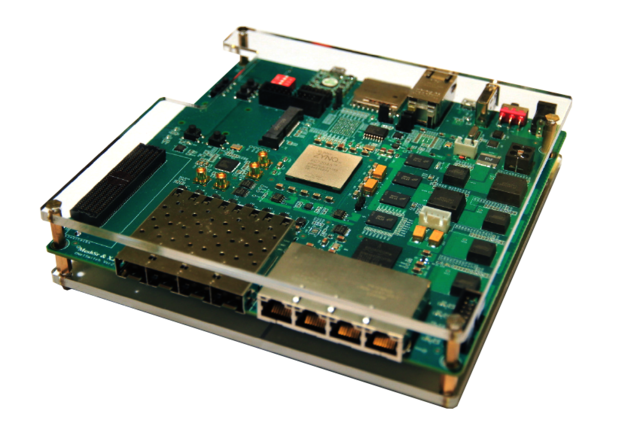
ONetSwitch45 is an All Programmable open networking innovation platform. ONetSwitch45 is based on the Xilinx Zynq-7000 SoC, adopts the Gigabit ports and the 10G ports, and can extend wireless or storage. Both its software and hardware can realize custom programming. Its reference designs are abundant and flexible, can be used to various researches on the evolution of network prototypes, and the development of customized network products. Especially, the features of the miniaturization and low power are adapted to the multi-node network tests and deployments.
Features
- General
Main Silicon XC7Z045-2FFG676 Power Supply DC 12V Primary Config. SD card Auxiliary Config. QSPI flash/JTAG
- Processing System
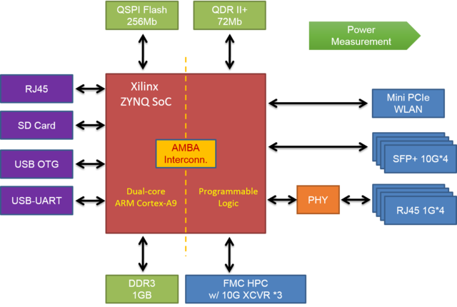
Processor Dual ARM Cortex-A9@800MHz Cache (L1)32KB Inst. + 32KB Data per core; (L2)512KB; (OCM)256KB DRAM DDR3 1GBytes Flash Quad SPI flash 256Mb DMA 8 channel (4 for Programmable Logic) Ethernet 1x GE RJ45 Peripherals USB / USB-UART / USB JTAG / SD card
- Programmable Logic
FPGA Logic 350K LCs, Kintex-7, ~5.2M ASIC gates Host I/F AMBA AXI4 interconnect, max 100Gbps between PS-PL SRAM QDRII+ 72Mb, 57.6Gbps@400MHz Ethernet 4x GE RJ45, 4x 10GE SFP+ Peripherals FMC HPC, including 3x 10Gbps XCVRs User IO user LEDs/push buttons/DIP switch Extension mini PCIe for wireless NIC or SSD
Block Diagram
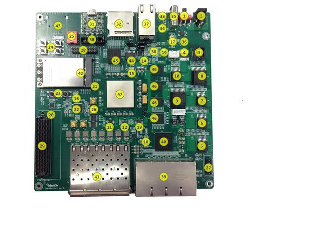
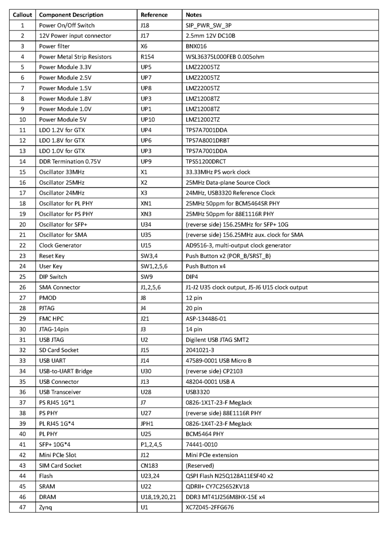
Board Layout
Specification
For details of the board hardware, please download the ONetSwitch45 Hardware User Guide.
Getting Started
1.Creat a New Partition on the SD card
2.Prepare boot files on the SD card
3.Set the SD card boot model
4.Setup a Serial Console
5.Power up and Running


